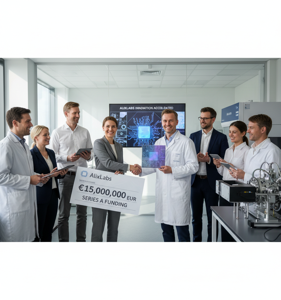
Lund, Sweden – [Date] – AlixLabs, the pioneering deep-tech semiconductor startup headquartered in Lund, Sweden, has announced the successful completion of a €15 million Series A funding round. The significant capital injection, which includes a strategic top-up from Finnish investor Stephen Industries, marks a pivotal moment for the company as it accelerates towards the commercialization of its proprietary Atomic Pitch Splitting (APS™) technology. This funding is ear-marked to facilitate beta testing with leading chipmakers by 2026, targeting full manufacturing deployment by 2027, promising a new era of precision in semiconductor fabrication.
The Imperative for Atomic Precision in a Shrinking World
The semiconductor industry is perpetually driven by Moore's Law, demanding ever-smaller and more powerful integrated circuits. However, conventional lithography techniques are reaching their physical limits, making the precise patterning of nanoscale features increasingly challenging and expensive. AlixLabs' APS™ technology addresses this critical bottleneck by enabling atomic-scale etching, offering a more controlled and cost-effective method for creating high-density semiconductor devices. This breakthrough is essential for the continued advancement of computing power, artificial intelligence, and a myriad of connected technologies.
Strategic Investment Fuels Commercialization Roadmap
The €15 million Series A round represents a strong vote of confidence from investors in AlixLabs' disruptive potential. While the full list of investors beyond Stephen Industries was not disclosed, their participation underscores the perceived value of APS™. The capital will be primarily allocated towards scaling up research and development efforts, expanding the engineering team, and establishing pilot production capabilities. AlixLabs’ ambitious timeline aims for beta testing within three years and mass production capabilities within four, indicating a clear, aggressive strategy to penetrate a highly competitive market where speed to innovation is paramount.
Impact on the Global Semiconductor Landscape
AlixLabs' APS™ technology could significantly impact the global semiconductor landscape by offering a vital solution to current patterning limitations. As chipmakers increasingly struggle with the economic and technical challenges of extreme ultraviolet (EUV) lithography, alternative or complementary technologies like APS™ become increasingly attractive. By enabling denser and more energy-efficient integrated circuits, AlixLabs could empower advancements in high-performance computing, memory solutions, and specialized processors for emerging fields like quantum computing and advanced IoT devices, potentially reducing manufacturing costs and accelerating product development cycles across the industry.
Expert Perspectives on the Deep-Tech Breakthrough
Industry analysts and semiconductor experts view AlixLabs' progress with considerable interest. Dr. Anya Sharma, a senior analyst at Tech Insights Group, commented, "The ability to achieve atomic-level precision in semiconductor manufacturing is the holy grail for continued scaling. AlixLabs' APS™ technology, if successfully commercialized on schedule, could provide a much-needed lifeline to chipmakers struggling with the economic viability of traditional lithography at advanced nodes. This funding round demonstrates significant investor confidence in their unique approach and the potential for a substantial return." The deep-tech nature of the innovation positions AlixLabs at the forefront of materials science and advanced manufacturing.
The Path Forward: From Labs to Fab
Looking ahead, AlixLabs' immediate priorities include expanding its intellectual property portfolio and forging strategic partnerships with major global semiconductor manufacturers. The company’s roadmap involves demonstrating the scalability and reliability of APS™ in real-world production environments during the planned beta testing phase in 2026. Successful validation will be crucial for securing long-term contracts and establishing APS™ as a standard in next-generation chip fabrication. The 2027 manufacturing deployment target signifies the company's commitment to translating groundbreaking research into tangible industrial impact, potentially reshaping how chips are made for decades to come.
Stephen Industries' Strategic Alignment
Stephen Industries' strategic investment not only provides crucial capital but also potentially opens doors for AlixLabs into new markets and strategic collaborations. As a Finnish investor, their involvement could facilitate partnerships within the Nordic and broader European tech ecosystems. This additional backing further solidifies AlixLabs' financial position and operational runway, enabling them to focus resources on scientific and engineering milestones required to bring APS™ from a cutting-edge laboratory concept to a fundamental industrial process.
Revolutionizing Miniaturization
Ultimately, AlixLabs' journey represents the relentless pursuit of miniaturization, a hallmark of the semiconductor industry. Its APS™ technology is poised to contribute significantly to this pursuit, offering a path to creating components that are not only smaller but also more powerful and efficient. The €15 million Series A is not merely an investment in a company; it is an investment in the future of electronics and the digital world the world relies upon.