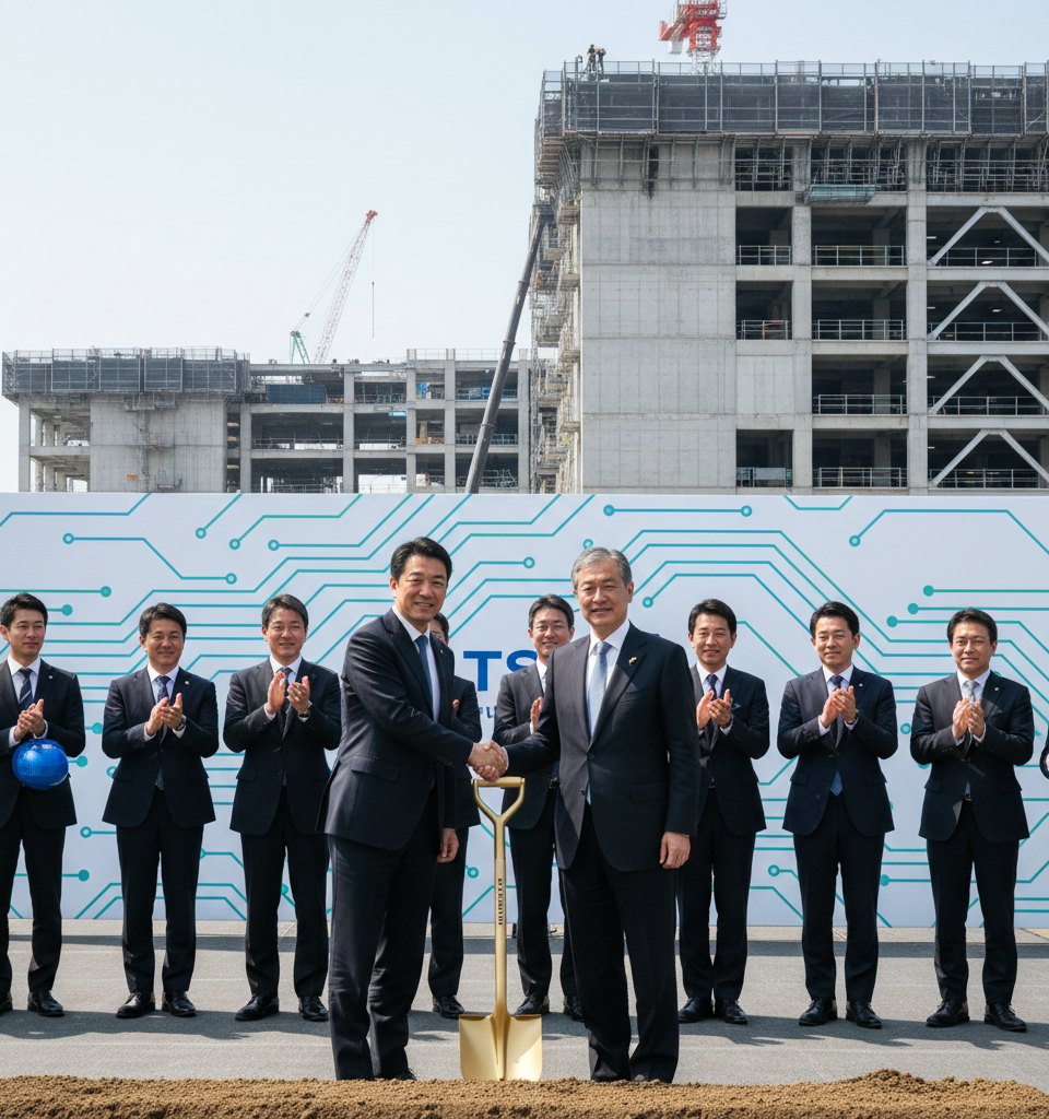
Sony Semiconductor Solutions Corporation (SSS), a subsidiary of the Japanese electronics giant Sony Group, is reportedly deepening its collaboration with Taiwan Semiconductor Manufacturing Company (TSMC), the world's leading independent semiconductor foundry. The partnership centers on a new, high-tech chip manufacturing plant under construction in Kumamoto Prefecture, Japan, with Sony aiming to leverage TSMC's advanced process technology to significantly enhance the production capabilities of its sophisticated image sensors. This move underscores Sony's commitment to maintaining its dominant position in the global image sensor market, particularly as demand surges for higher-resolution cameras in smartphones and autonomous vehicles.
Context and Background
Sony has long been a powerhouse in the image sensor market, commanding an estimated 42% global share as of late 2023, far ahead of competitors like Samsung and OmniVision. Their sensors are integral to a vast array of products, from Apple's iPhones to advanced industrial cameras. However, the manufacturing of these highly complex components requires increasingly sophisticated semiconductor processes, an area where TSMC excels. The decision to co-locate a facility in Japan, backed by substantial Japanese government subsidies, aligns with a broader global trend of diversifying semiconductor supply chains and bringing critical manufacturing closer to end-market consumption. This collaboration is a strategic response to the intense capital expenditure and technological expertise required to stay at the forefront of chip innovation.
Key Details of the Collaboration
While specific financial terms of Sony's direct investment have not been fully disclosed, TSMC's initial Kumamoto fab, known as Japan Advanced Semiconductor Manufacturing (JASM), involves an investment of approximately $8.6 billion and commenced construction in April 2022. The Japanese government is providing roughly 40% of the initial investment. Sony is expected to be a key customer and potentially an equity partner in JASM alongside Denso, focusing on the production of image sensor logic chips using mature 12/16 nanometer and 22/28 nanometer process technologies. This partnership extends beyond merely being a customer; it signifies a strategic alignment to co-develop and optimize manufacturing processes specifically for advanced image sensors, ensuring a stable and technologically superior supply chain for Sony's growing needs.
Industry and Market Impact
This collaboration sends significant ripples through the global semiconductor and image sensor industries. For Sony, it secures access to TSMC's cutting-edge fabrication technology, allowing them to produce image sensors with higher pixel counts, superior low-light performance, and faster processing speeds, crucial for markets like AR/VR, automotive ADAS (Advanced Driver-Assistance Systems), and high-end smartphones. For TSMC, it diversifies its customer base and solidifies its position as the favored foundry partner for specialized components.
The Kumamoto facility also bolsters Japan's ambitions to revitalize its domestic chip manufacturing capabilities, reducing reliance on overseas production and fostering economic growth in the region. This move could also intensify competition, pushing other image sensor manufacturers like Samsung to seek similar strategic foundry partnerships or significantly ramp up their own in-house capabilities.
Expert Perspective
Industry analysts view this partnership as a shrewd move for both companies. "Sony leveraging TSMC's manufacturing prowess is a natural evolution given the increasing complexity of imaging chips," stated Dr. Akira Sugiyama, a Tokyo-based semiconductor analyst. "It allows Sony to focus on its core strengths in design and innovation, while outsourcing the capital-intensive manufacturing to the undisputed leader." He added that the Japanese government's involvement highlights the strategic importance of semiconductor independence. "This isn't just about an individual company's success; it's about national technological sovereignty, especially in critical components like image sensors that power the digital economy." The move positions Sony to maintain its lead in the next wave of imaging technology innovation.
What's Next
The construction of the JASM Kumamoto plant is progressing rapidly, with production anticipated to begin by late 2024. As the facility scales up, observers will be keen to see the tangible benefits for Sony's image sensor product roadmap. Future developments could include a deeper co-development of process technologies specifically optimized for stacked image sensors and potentially expanding the scope to include more advanced process nodes. The success of this Japanese venture could also influence TSMC's decisions regarding additional international expansion, potentially leading to similar partnerships in other regions. Ultimately, this collaboration is a clear indicator of the increasing interdependence and strategic alliances forming within the high-stakes semiconductor industry, driven by escalating R&D costs and geopolitical considerations.